
A cascode amplifier, a two-stage circuit used in analog electronics, provides higher gain, wider bandwidth and improved input and output impedance.
Hence, combining a common-source and common-gate amplifier reduces the Miller effect and improves stability, this design also finds use in RF amplifiers, high-speed op-amps, and instrumentation circuits.
This article for Simple Cascode Amplifier Circuit teaches us about FET Cascode amp how it works, formulas, real circuit making and the tips required while making.
Circuit Working:
Working of FET cascode amplifier circuit:
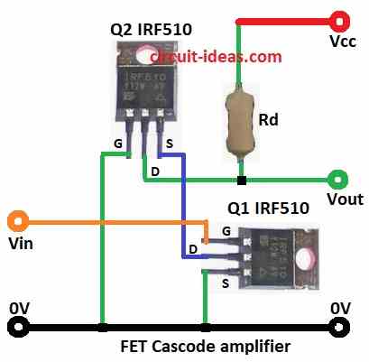
The cascode amplifier circuit with FET has two parts: the first part uses a common-source FET, where Vin goes to its gate and the second part uses a common-gate FET, which the first stage drives.
Rd acts as the drain resistor in the output stage and Vout comes from the drain of Q2.
Q2 gate is at ground so Q2 source and Q1 drain stay almost at same voltage and then Q2 gives low input resistance to Q1, as a result, this lowers gain of Q1, but also reduces Miller effect for better bandwidth.
After that, Q2 makes up for Q1 gain loss so total gain stays good and hence, Q2 is not much affected by Miller effect.
Capacitance charge/discharge goes through Rd and load which affects only a very high frequencies.
Formulas:
Here are basic formulas for FET Cascode amplifier:
Voltage Gain (Av):
Av = gm × Rd
where,
- gm is FET transconductance
- Rd is drain resistor of Q2
Input Impedance (Zin):
where,
Zin = Rg1
- Rg1 is gate resistor of Q1
Output Impedance (Zout):
Zout = Rd
where,
- Rd is drain resistor of Q2
Bandwidth (BW):
BW goes up because Miller effect is small with following formula:
BW ∝ 1 / (Cgd × Av)
where,
- Cgd is gate-drain capacitance
Working of realistic cascode amplifier circuit:
Parts List:
| Components | Values | Quantity |
|---|---|---|
| Resistors (All resistors are 1/4 watt unless specified) | 10M | 1 |
| 330Ω | 1 | |
| 3.9k | 1 | |
| 27k | 1 | |
| 10k | 1 | |
| Capacitors | Electrolytic 1µF | 1 |
| Semiconductors | FET IRF510 | 2 |
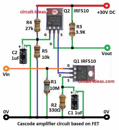
Real FET cascode amp circuit shown is above.
R4 and R5 make voltage divider and give bias to Q2, R3 is drain resistor of Q2 and controls drain current and R2 is source resistor of Q1.
C1 is bypass capacitor for R2 which improves the gain and R1 keeps gate of Q1 at zero volts when there is no input signal.
How to Build:
To build a Simple Cascode Amplifier Circuit follow the below mentioned connections steps:
- First, Q1 gate pin connect to Vin through R1 and also to GND.
- Next, Q1 source pin connect to GND through R2
- Also Q1 source pin connect C1 from this pin to GND of bypass capacitor.
- Then Q1 drain pin connects to Q2 source.
- After that, Q2 gate pin connects to (+) of C2 and (–) of C2 to GND.
- Now Q2 gate pin also connect R4 to +V and R5 to GND of voltage divider bias.
- Further Q2 drain pin connects to Vout through R3 to +V
- Finally, Q2 source pin connects to Q1 drain pin.
Conclusion:
Overall, Simple Cascode Amplifier Circuit is smart circuit, it gives high gain and works on wide frequencies and has less problem from Miller effect.
Also, it mixes common source + common gate and keeps signal clean which is good for high speed, hence, with right biasing and capacitors the circuit becomes strong and stable.
Moreover, it is best for RF, fast op-amps and accurate systems where bandwidth matters.