
In my previous article for Switch Selectable Four Frequency Pulse Generator Circuit i selected the frequency using manual switches; however, this circuit replaces manual switching with electronic switching by using the CD4066B quad bilateral switch, which the 555 timer controls automatically.
The CD4066 is a quad bilateral switch IC that contains four independent analog switches in a single chip.
Each switch can pass analog or digital signal in both directions, which means signal can flow from either side.
IC CD4066 works together with IC 555 timer, this 555 timer produces output pulses and these pulses control the switching action of CD4066.
This CD4066 analog switch with a 555 timer circuit is useful for signal routing, audio switching, digital selection and simple logic control, also it operates with low power, uses low cost components, and offers an easy design to build.
Circuit Working:
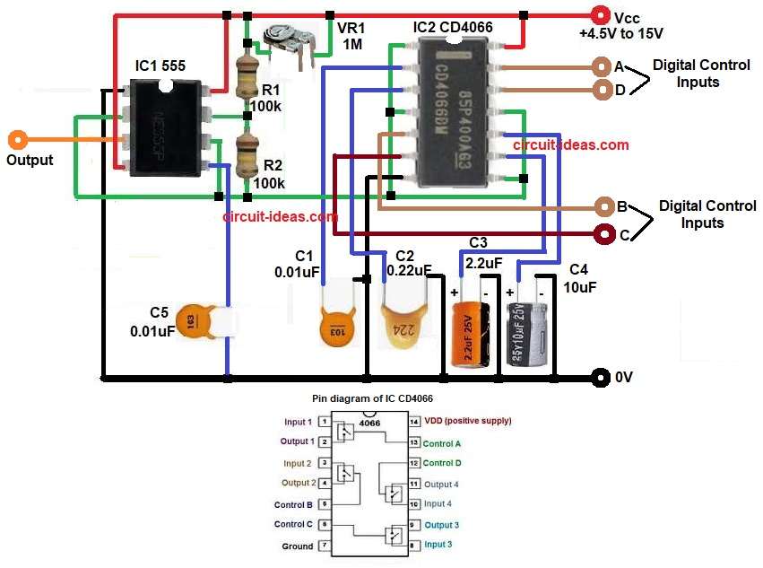
Parts List:
| Components | Values | Quantity |
|---|---|---|
| Resistors | 100k | 2 |
| Preset 1M | 1 | |
| Capacitors | Electrolytic 2.2uF 25V, 10uF 25V | 1 |
| Ceramic 0.01uF | 2 | |
| Ceramic 0.22uF | 1 | |
| Semiconductors | IC CD4066 | 1 |
| IC 555 Timer | 1 | |
| Power Supply 4.5V to 15V DC | 1 |
To begin with, the circuit start first with power supply given from 4.5V to 15V; the 555 timer works as astable multivibrator and therefore, it generates square wave output at pin 3.
The frequency of oscillation depends on VR1, R1, R2 and timing capacitor.
When output of 555 becomes HIGH then corresponding control pin of CD4066 becomes HIGH; as a result a selected analog switch inside CD4066 turns ON and so input signal passes through the switch.
However, when the 555 timer output becomes LOW, the control pin also goes LOW, which turns the switch OFF and disconnects the signal path.
Each digital input (A, B, C, and D) controls an individual switch section, while the timing capacitors (C1, C2, C3, and C4) provide signal shaping and filtering.
Thus, circuit allows digital control of analog signals.
How to Build:
To build a CD4066 Analog Switch with 555 Timer Circuit follow the below connection steps:
- First, start circuit and collect all parts as shown in circuit diagram.
- Now take IC1 555 timer, pin 1 connect to GND.
- Then pin 2 connect to pin 6 same IC.
- Next, pin 3 is output.
- Also pin 4 and pin 8 connect to VCC (4.5V to 15V).
- Further, pin 5 connect to capacitor C5. Other side capacitor to GND.
- Pin 7 connect between R1 and VR1, also connect resistor R2 from pin 7 to pin 2.
- Now take IC2 CD4066, pin 14 VDD connect to VCC.
- Pin 7 VSS connect to GND.
- Switch 1 of IC2: pin 1 and pin 2 are analog pins.
- Pin 13 is control pin.
- Switch 2 of IC2: pin 4 and pin 3 are analog pins.
- Pin 5 is control pin.
- Switch 3 of IC2: pin 8 and pin 9 are analog pins.
- Pin 6 is control pin.
- Switch 4 of IC2: pin 11 and pin 10 are analog pins.
- Pin 12 is control pin.
- Finally, pin 2, pin 3, pin 9 and pin 10 connect together in parallel.
- Connect one side of capacitors C1 to C4 to these pins and other side of all capacitors connect to GND.
Conclusion:
Overall, CD4066 quad bilateral switch is very useful IC, which allows easy digital control of analog signals and when combined with 555 timer, it gives automatic switching operation.
The CD4066 Analog Switch with 555 Timer Circuit is simple, construction is easy, cost is low and also power consumption is very small.
Therefore, this circuit is good for beginners and practical electronics projects, as it is suitable for audio switching, signal control and experimental work.