Simple Buck Converter Circuit for Converting 12V to 3V also called step-down converter is common in electronics; it takes high DC voltage and makes it lower, like a valve but for voltage.
Additionally, phones and laptops use this type of circuit to convert a 12V battery supply into lower voltages, such as 3V, for smaller components.
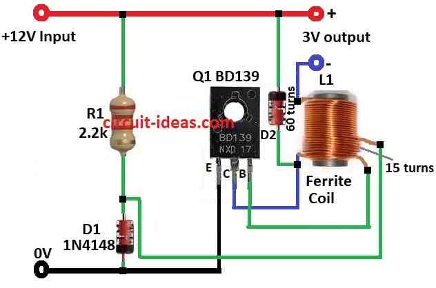
Circuit Working:
Parts List:
| Components | Values | Quantity |
|---|---|---|
| Resistor | 2.2k (1/4 watt) | 1 |
| Semiconductors | Transistor BD139 | 1 |
| Diodes 1N4148 | 2 | |
| Ferrite rod, 10mm diameter, 15mm length, wound as follows:- 60 turns of 0.25mm wire. Additional 15 turns on top of the 60 turns, using the same 0.25mm wire | 1 |
To begin with, 12V input comes from left side of circuit (see diagram).
First, when transistor Q1 turns ON current goes from 12V through coil L1 then through resistor R1 2.2k and to ground and then coil L1 resists sudden change in current so voltage across it stays high at first.
Hence, this makes output voltage spike and it can also go higher than 12V which may hurt some circuits.
Diode D1 is in reverse bias across coil and when Q1 turns OFF coil still wants to keep current flowing.
Now current goes through D1 with now forward biased and then it goes to ground and then this stops voltage from dropping too fast and keeps output voltage more stable.
Q1 is a BJT transistor and the signal voltage controls its base, additionally, resistor R1 provides the base bias for Q1.
Here it is 2.2k ohm, right value depends on transistor and needed output voltage.
Diode D2 is a Schottky diode across output and this Schottky has low voltage drop which helps in efficiency; but maybe not needed if output current is low.
Formulas:
Important formula for Buck Converter:
Vout = Vin × D
where:
- Vout is output voltage here in this circuit it is 3V
- Vin input voltage and here it is 12V
- D is duty cycle where how long transistor Q1 stays ON
Duty cycle D = Ton / Ts
- Ton is the ON time of Q1
- Ts is the Total time of one full cycle ON + OFF
So D is just % of time Q1 is ON.
Hence, changing the pulse frequency from driver circuit and changes D; higher D means Q1 stays ON longer and output voltage goes closer to Vin.
How to Build:
To build a Buck Converter Circuit for Converting 12V to 3V follow the below mentioned steps:
- First, connect emitter of transistor Q1 to ground, connect collector of Q1 to one end of coil L2 and other end of L2 goes to 3V output and then connect base of Q1 to coil L1.
- Now put resistor R1 and diode D1 between positive and negative supply and the add diode D2 from base of Q1 to positive supply.
Safety Note:
- Be careful while working with electronics and if anyone is new then ask help from someone experienced.
Conclusion:
To conclude, this Simple Buck Converter Circuit for Converting 12V to 3V is like small transformer for DC, as it turns 12V into 3V.
Also, it is useful for powering small devices from big power source and therefore these type of circuits are very common in electronics.
Leave a Reply