Audio Signal Distributor Circuit with Three Outputs is used to split one audio signal into three outputs with no sound quality loss.
This circuit uses NE5532 op-amp and BC337, BC327 transistors.
It send same audio to three outputs.
The circuit is useful for sound system, headphone splitter or sending sound to many rooms.
Circuit Working:
Parts list:
| Component | Specification | Quantity |
|---|---|---|
| Resistors (All resistors are 1/4 watt unless specified) | ||
| 560k | 1 | |
| 1k | 1 | |
| 2.2k | 1 | |
| 2.7k | 2 | |
| 330Ω | 3 | |
| Potentiometers 100k | 2 | |
| Capacitors | Electrolytic 100μF 25V | 4 |
| Semiconductors | IC NE5532 | 1 |
| Transistors BC337, BC327 | 1 each | |
| Zener diode BZX79C18 | 2 |
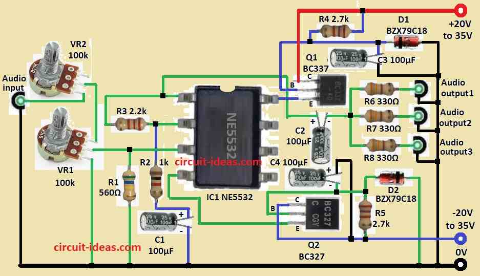
Audio signal come in through input and goes through resistors R1, VR1, VR2 to match impedance and give bias.
Capacitor C1 block DC from going into op-amp.
IC1 NE5532 work as buffer amp and audio goes in pin 3 of non-inverting pin, output come from pin 1.
Capacitor C2 remove DC noise and keep signal clean.
Zener diodes D1, D2 and resistors R4, R5 give stable positive and negative voltage for op-amp and transistors.
This make circuit work good with input voltage from +20V to +35V.
Op-amp output goes to three outputs Audio 1, 2, 3 using resistors R6, R7, R8 to split signal equal.
Transistors Q1 BC337 and Q2 BC327 boost and stabilize current for both positive and negative signal.
Capacitors C3, C4 help smooth audio more and make quality better.
Formulas with Calculations:
To make our own Audio Signal Distributor Circuit then use these formulas:
Voltage Regulation:
Zener voltage (Vz) = 18V for D1, D2
Resistor for zener:
R4 = (Vin – Vz) / Iz
Example: Vin = 20V, Iz = 2.7mA
R4 = (20 – 18) / 0.0027 = 740Ω = 2.7k
Input Impedance (Zin):
Zin = R1 || (VR1 + VR2)
Example: R1 = 560k, VR1 = 100k, VR2 = 100k
Zin = 1 / [(1 / 560k) + (1 / 200k)] = 50k
Op-Amp Gain:
NE5532 used in unity gain mode:
Vout = Vin
Output Current (Iout):
Based on resistors R6, R7, R8
Example: Vout = 1V, R6 = 330Ω
Iout = 1 / 330 = 3.03mA
How to Build:
To build a Audio Signal Distributor Circuit with Three Outputs following steps we need to follow while assembling:
- Collect all parts shown in circuit diagram.
- Pin 1 of IC1 NE 5532 go to positive side of C2.
- Negative side of C2 go to Audio Output1, 2, 3 through resistors R6, R7, R8.
- Pin 1 also connect to pin 2 with resistor R5.
- Pin 2 connect to GND through resistor R2 and capacitor C1.
- Pin 3 connect to middle leg of VR1.
- Top leg of VR1 go to middle leg of VR2 and last leg go to GND.
- Resistor R1 go from pin 3 to GND.
- Middle leg of VR2 go to center of VR1 and other leg go to Audio input and GND.
Power Connection:
- Pin 4 of IC1 connect to emitter of Q2.
- Collector of Q2 goes to -VCC (–20V to –35V).
- Base of Q2 goes to negative of C4 and positive of C4 goes to GND.
- From Q2 base connect diode D2 to GND and then resistor R5 to –VCC.
- Pin 8 of IC1 go to emitter of Q1 and collector go to +VCC (+20V to +35V).
- Base of Q1 goes to positive of C3 and negative of C3 to GND.
- From +VCC connect resistor R4 and diode D1 to GND.
Conclusion:
This Audio Signal Distributor Circuit with Three Outputs split one audio signal into 3 outputs with no sound loss.
It uses NE 5532 op-amp to keep sound clean.
Transistor stage give enough power for speakers or devices.
It is simple to make with strong design and is good for home and professional audio use.
Leave a Reply