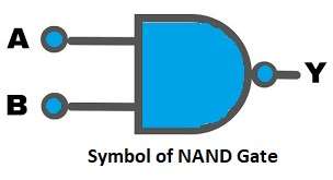
Logic NAND Gate Circuit using Transistors is very important in digital logic, as it work opposite of AND gate.
Output is HIGH when any input is LOW.
People call the NAND gate a universal gate because it can implement all other basic logic gates, including AND, OR, and NOT.
Truth Table for Logic NAND Gate:
| Input A | Input B | Output (Y = NOT (A AND B)) |
|---|---|---|
| 0 | 0 | 1 |
| 0 | 1 | 1 |
| 1 | 0 | 1 |
| 1 | 1 | 0 |
A NAND gate gives output 1 for all input combinations except when both inputs are 1 and when both A and B are 1 then output becomes 0.
Symbol for Logic NAND Gate:
Circuit Working:
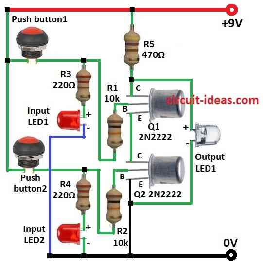
Parts List:
| Components | Values | Quantity |
|---|---|---|
| Resistors | 10k 1/4 watt | 2 |
| 220Ω 1/4 watt | 2 | |
| 470Ω 1/4 watt | 1 | |
| Semiconductors | Transistors 2N2222 | 2 |
| Input LEDs 5mm 20mA | 2 | |
| Output LED 5mm 20mA | 1 | |
| Push buttons | 2 |
Power to First Transistor Q1:
First, Vcc supplies power to the collector of Q1, additionally, resistor R5 limits and controls the current flowing through Q1.
Connecting the Transistors:
Then Q1s emitter goes to Q2s collector and this link helps NAND gate to work.
Getting the Output:
Now Q1s collector also goes to output LED1 and this is where final output signal comes.
Inputs Handling:
First input push button1 goes to Q1s base through resistor R1 and this R1 limits current to base.
Same for second input push button2, it goes to Q2s base with resistor R2.
Why NAND is Different Than AND:
AND gate takes output from Q2s emitter and NAND gate takes output from Q1s collector and then this small change makes logic different.
Output Behavior:
If both inputs are HIGH, we press both push buttons and turn ON both Q1 and Q2.
Current flows to ground instead of the output, causing the output LED to indicate a LOW state.
However, if either input goes LOW, at least one push button remains unpressed, which turns OFF the corresponding transistor.
As a result, current cant go to ground and so it flows to output and hence output LED gets HIGH.
Summary:
NAND gate gives HIGH output when any input is LOW.
Formulas:
Transistor Base Resistor:
To turn ON transistor well find base resistor Rbase:
Rbase = (Vin − Vbe) / Ib
where,
- Vin is the input voltage which is mostly 9V
- Vbe is the base-emitter voltage to about 0.7V for 2N2222
- Ib is the base current to make transistor ON for saturated
LED Current Limiting Resistor:
To stop too much current in LED use RLED:
RLED = (Vsupply − VLED) / ILED
where,
- Vsupply is the power voltage for 9V
- VLED is the LED forward voltage for around 2V
- ILED is the LED current for about 20mA for normal LED
Pull-Up Resistor for Push Buttons:
To keep the logic level HIGH when we do not press the button then use a pull-up resistor.
Rpull-up = Vsupply / Ipull-up
where,
- Ipull-up the current needed when button is open
We can use 2N2222 transistors, resistors, LEDs and push buttons to make NAND gate, hence, change values as needed for our own circuit.
How to Build:
To build a Logic NAND Gate Circuit using Transistors follow the below mentioned steps for connections:
- First, connect Q1 collector to positive (Vcc) through resistor R5, connect Q1 base to push button1 through resistor R1 and then connect Q1 emitter to Q2 collector.
- Next, connect output LED1 anode between Q1 collector and R5 and connect LED1 cathode to ground, connect Q2 base to push button2 through resistor R2 and then connect Q2 emitter to ground.
- Between push button1 and R1 add resistor R3 and input LED1 and again between push button2 and R2 add resistor R4 and input LED2.
Extra Info:
- Resistor values may change with transistor type and power supply, therefore, this simple circuit can change design if needed.
- Also, be careful when working with electronics and follow safety rules.
Conclusion:
Overall, this Logic NAND Gate Circuit using Transistors is small but useful, as it gives HIGH output only when any input is LOW; also its very important part of digital logic systems.
Leave a Reply