This article make it easy to build one Modified Sine Wave Inverter Circuit
It uses two small chips IC 4017 and IC 555 to make square wave look more smooth.
The circuit also show all parts and how wires connect so we can understand better.
Understanding Modified Sine Wave Inverter:
Battery power can change to home power using different types of inverters.
Modified sine wave inverter is better than basic one that make blocky wave.
It makes smoother wave for some machines.
Big difference is that normal switch go up and down fast but modified sine wave stop at zero for little time before changing the direction.
Comparing Square Wave and Modified Sine Wave Inverters:
Square wave inverter work like fast ON/OFF light switch.
It turn electricity ON and OFF very quickly which can be bad for some machines.
Modified sine wave inverter is more smooth like dimmer switch.
It stops at zero for small time before changing the direction.
This make power more clean and less trouble for devices.
It not perfect like real sine wave but much better than square wave.
Understanding the Modified Inverter Circuit:
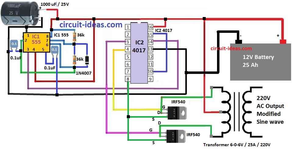
Parts List:
| Component | Quantity |
|---|---|
| Resistors | |
| 36k 1/4 watt | 2 |
| Capacitors | |
| PPC 0.1µF | 2 |
| Electrolytic 1000µF 25V | 1 |
| Semiconductors | |
| Diode 1N4007 | 1 |
| IC 4017 | 1 |
| IC 555 | 1 |
| MOSFET IRF540 | 2 |
| Transformer 6-0-6V / 25A / 220V | 1 |
| Battery 12V 25Ah | 1 |
The modified inverter make modified sine wave at output it have different parts:
Oscillator Stage (IC 555):
This part is very important as it makes clock signal for inverter and is like heart of a circuit.
For this we use IC 555 as oscillator.
We want to make 200Hz square wave with 50% duty cycle.
Then we use IC 4017 to divide it by 4 and get 50Hz AC modified sine wave.
The frequency of IC 555 is found by using the following formula:
Formulas and Calculations:
Below are formulas and calculation for making Modified Sine Wave Inverter:
Frequency = 1.44 / (R1 + R2) × C
Duty Cycle = R1 / (R1 + R2)
We use values from circuit diagram to put in formula:
Frequency = 1.44 / (36000 + 36000) × 0.1 × 10⁻⁶ = 200 Hz
Duty Cycle = 36000 / (36000 + 36000) = 0.5
Duty Cycle = 0.5 × 100% = 50%
Let us analyze this on the scope:
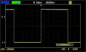
About component limits the scope reading shows circuit is working close to expected values.
Important Note:
The 0.1uF capacitor at pin 5 of IC 555 is very important it helps to stop outside noise.
If we do not use this capacitor frequency and duty cycle can change from what we calculate.
Wave Shaping Stage (IC 4017):
In this part we give 50Hz 50% duty signal to IC 4017 and this chip is called decade counter which help to make modified sine wave.
IC 4017 has 10 output pins and one input pin (pin 14).
When clock signal connects to pin 14 each output pin turns ON one by one.
For example: after 5 clock signals, pin 5 output becomes active and others stay OFF.
Pin 15 is a reset pin and it can bring count back to 0 if we do not use all 10 outputs.
In our circuit we only use 4 output pins: pin 3, 2, 4 and 7 (Q0, Q1, Q2, Q3).
Pin 15 is connected to Q4 of pin 10 so only pin 3, 2, 4 and 7 stay active and other outputs stay OFF.
We give 200Hz signal to pin 14 of clock pin of IC 4017.
From all outputs we only use two: pin 3 (Q0) and pin 4 (Q2).
Other pins are not connected.

Modified sine wave is taken from pin 3 and 4.
This wave will connect to MOSFETs to make stronger.
We can see this wave using oscilloscope.