In this article we will discuss about Dual 35V 300 Watt SMPS Circuit which gives two 35V power output and are used for high power things.
Also, circuit work fast and save energy and is good for big electronic project.
What is a Dual 35V 300 Watt SMPS Circuit:
A strong dual 35V 300 Watt SMPS circuit must be made properly and we should check power, resistance and voltage to make it work best.
This Dual 35V 300W SMPS circuit can give total 300 watt power and two outputs with +35V and -35V.
Furthermore, these circuits are mostly used for audio amplifier and other devices which need steady high power DC voltage.
Circuit Working:
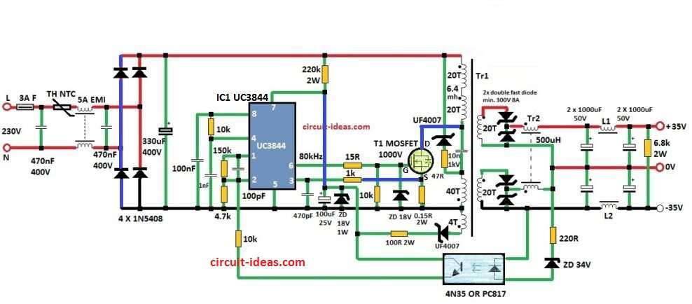
Parts List:
- Printed Circuit Board
- MOSFETs SPB17N80C3
- IC UC3844
- Heat sinks
- Resistors, capacitors and diodes
- Power supply components (transformer, rectifier)
- Voltage regulators
- Wiring and connectors
- Multimeter and oscilloscope
- Soldering iron and solder
- Insulating materials
First, we need to use MOSFETs with low ON resistance (Rds ON) to stop power loss and for 300W power supply Rds ON should not be more than 0.8 ohm.
We can make resistance lower by using more MOSFETs in parallel and very important part is voltage should be between drain and source UDS and UDS should be 900 to 1000V and 800V is okay only in bad condition.
Also, we must be very careful to stay in safe voltage limit.
Hence, when picking power parts for this dual 35V 300W SMPS we think about MOSFETs or IGBTs, but 600V IGBTs maybe not good for this, IGBTs with 1200V are safer but they work slower.
In actual test MOSFET SPP17N80C3 with very low 0.25 ohm resistance works better than IGBT BUP213 which makes more power loss.
Formulas:
Formulas for Dual 35V 300 Watt SMPS Circuit:
Rtotal = Rdson / N
This formula help to find total resistance (Rtotal) when N MOSFETs are connected in parallel and they are ON.
Simple Idea:
Rdson means resistance between drain and source when one MOSFET is ON.
Low Rdson is good and on less power is lost with more efficient.
N is how many MOSFETs we use in parallel, in parallel voltage is same for all but resistance goes lower.
How Formula Work:
Think each MOSFET has same Rdson and if we connect many in parallel it makes more paths for current.
So total resistance Rtotal becomes lower.
Use formula: divide Rdson by number of MOSFETs (N) → get Rtotal.
Transformer and Inductor Details:
Tr1 is main transformer which uses ferrite core EE type with no gap the core area is between 90 to 140 mm².
Tr2 is inductor and it has 80 turns made using two wires together and wire size is 0.8 to 1 mm.
Core is big iron powder toroid (yellow-white or green-blue type from old PC power supply).
Inside size 14 mm and outside 27 mm with height 11 mm.
L1 is 2 inductors and each 20 turns using 0.8 mm wire on ferrite rod from PC power supply.
This project is not good for beginners as Dual 35V 300 Watt SMPS uses high voltage from mains which is very dangerous and if design is not right then mains voltage can go to output which might be very risky.
Even after power is OFF big capacitors may still have dangerous voltage.
Do this project at ones own risk and the writer is not responsible for any damage or injury.
Making high power switching supply needs care and many steps, so below is one important way to build 300W switching power supply using MOSFETs in parallel, but design can change based on parts and idea used.
How to Build:
To build a Dual 35V 300 Watt SMPS Circuit follow the below mentioned steps for connections:
- First, choose MOSFETs like SPP17N80C3 which have low ON resistance and good for high power use.
- Based on power needed calculate how many MOSFETs we need.
- To make ON resistance lower connect MOSFETs in parallel.
- Use gate resistors to balance voltage and share load equal between all MOSFETs.
- Also, pick a transformer that can give right power and voltage.
- Add a rectifier circuit to change AC to DC.
- Use voltage regulator to keep output voltage steady.
- Use feedback circuit to control and change the output properly.
- Then, put heat sinks on MOSFETs to throw out heat.
- Be sure thermal contact is good so parts do not get too hot.
- While making PCB layout think about signal lines, heat flow and part positions.
- Use software tool or ask help to design PCB correctly.
- After that, place all parts on PCB same as in design.
- Solder all wires and parts well for strong connection.
- Use multimeter and oscilloscope to test circuit and check voltage and wave shapes.
- Finally, look for short circuits or broken wires before turning power ON.
Safety Measures:
Use safety steps to protect from overheating, overvoltage and overcurrent.
To stop people from touching live parts by mistake then put the circuit inside a safe box or case.
Conclusion:
This Dual 35V 300 Watt SMPS Circuit give basic idea but some things can change based on parts and design we choose.
Always read datasheets and test everything carefully and follow safety rules while making the circuit and if not sure about the circuit connections ask help from expert to stay safe.
Leave a Reply