Frequency to Voltage Converter Circuit using IC TC9400 is useful in signal work, motor speed control and sensor connect.
It takes frequency signal and gives voltage output and this helps to read and use frequency as voltage in many ways.
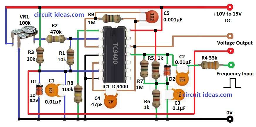
Also, the circuit operates from a 10–15 V DC power supply, the circuit diagram uses the TC9400 chip as an FVC with a single power source and the output voltage depends on the input frequency.
Furthermore, TC9400 is good chip and gives accurate change from frequency to voltage or opposite and it changes input frequency to matching DC voltage.
Circuit Working:
Parts List:
| Components | Values | Quantity |
|---|---|---|
| Resistors (All resistors are 1/4 watt unless specified) | 470k | 1 |
| 33k | 1 | |
| 100k | 1 | |
| 10k | 2 | |
| 1k | 2 | |
| 1M | 2 | |
| Preset 100k | 1 | |
| Capacitors | Ceramic 0.01µF | 2 |
| Ceramic 0.1µF | 1 | |
| Ceramic 47pF | 1 | |
| Ceramic 0.001µF | 1 | |
| Semiconductors | IC TC9400 | 1 |
| Zener Diode 6.2V | 1 | |
| Diode D2 = 1N914 | 1 |
First, frequency signal goes to Frequency IN pin (Pin 11) and R4 and C2 clean noise from signal and D2 helps shape signal right.
Then TC9400 IC turns frequency into voltage by making matching current and R9 and C5 set time constant inside IC and C4 which is C ref keeps reference voltage steady.
After that, output voltage comes from Voltage OUT pin and matches input frequency and VR1 adjusts offset voltage for calibration.
Now R4, C2, D2 fix input waveform before IC uses it and R5 and R7 pull signal level down as needed, then signal at Pin 11 becomes pulse signal for IC to convert.
Also, VR1 and R2 make adjustable voltage divider and sets reference voltage and this tuning ensure output is 0V or set value when there is no input frequency.
R8 R bias gives bias current for comparator in IC and R9 R int and C5 C int control how fast frequency turns into voltage and big R9 is slow but with smooth response and small R9 is fast but it may give bumpy output.
C5 with R9 sets integration time and big C5 is more stable but slow and small C5 is fast but maybe unstable output; but together R9 and C5 decide voltage stability and speed of response.
Formulas with Calculations:
Formula for FVC using TC9400:
Vout = K × fin
where:
- K is the constant which depends on R9, C5 and IC inside
- fin is the input frequency
Design idea:
More frequency means more voltage and less frequency means less voltage
Example:
If fin = 10 kHz, and K = 0.01 V/Hz:
Vout = 0.01 × 10,000 = 100V
But in actual circuit, output voltage is usually 0V to 10V or 0V to 5V, so we need to pick right parts to stay in range.
How to Build:
To build a Frequency to Voltage Converter Circuit using IC TC9400 follow the below mentioned steps:
- First, gather all parts as shown in circuit diagram.
- Next, pin 1 of IC1 TC9400 connect to GND through R8
- Then pin 2 connect to GND through R2 and VR1 preset
- After that, pin 3 connect to one end of R9 and other end of R9 connect to pin 12
- Also, pin 4 and pin 7 connects to GND
- Now pin 5 connects to one end of C4 and other end of C4 goes to pin 3
- Further, Pin 6 connects to one end of R1 and other end of R1 goes to pin and also connect C1 and D1 from pin 6 to GND
- Pin 11 connect to Frequency IN through C2 and R4, pin 12 connect to Voltage OUT through C5 and R9 and pin 14 connect to V+ from 10V to 15V DC
- Now R7 connects between junctions of R5 and R6.
- Finally, D2 cathode connect to pin 11 and anode connect one end of C3 and other end of C3 goes to GND
Conclusion:
To conclude, this Frequency to Voltage Converter Circuit using IC TC9400 converts input frequency to matching voltage, hence, change resistor and capacitor values to fit our need.
Moreover, if calibrated well it gives correct and steady voltage and also the circuit is good for analog signal systems using frequency.