XNOR gate is one of the basic logic gates, as it gives HIGH output when both inputs are same.
If both inputs are 0 or both are 1, the output becomes 1 and if one input is 0 and the other is 1, the output becomes 0; for this reason, the gate is also referred to as an ‘Equivalence Gate’.
In addition, this Logic XNOR Gate Circuit with Transistors is interesting to make.
Truth Table for Logic XNOR Gate:
| Input A | Input B | Output Y |
|---|---|---|
| 0 | 0 | 1 |
| 0 | 1 | 0 |
| 1 | 0 | 0 |
| 1 | 1 | 1 |
Output Y is HIGH (1) when both inputs A and B are same (00 or 11) and output Y is LOW (0) when inputs are different (01 or 10).
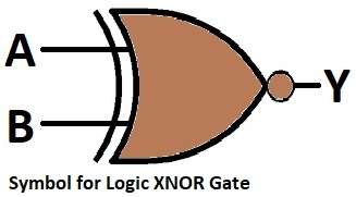
Symbol for Logic XNOR Gate:
Circuit Working:
Parts List:
| Components | Values | Quantity |
|---|---|---|
| Resistors | 4.7k 1/4 watt | 2 |
| 10k 1/4 watt | 4 | |
| 2.2k 1/4 watt | 1 | |
| Semiconductors | Transistor BC547 NPN | 5 |
| Power Supply +5V DC | 1 |
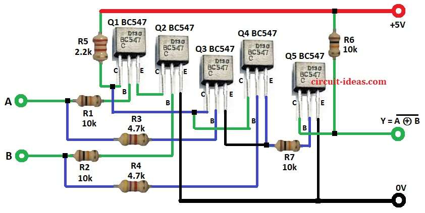
In the above circuit diagram when A and B both are LOW then Q1 and Q2 are OFF; then Q3 and Q4 also stay OFF.
Then Q5 get base current through R6 and R7 and output Y is HIGH.
When A and B both are HIGH then Q1 and Q2 turn ON and they give base signal to Q3 and Q4 and both turn ON.
Then Q4 ground the base of Q5 and so Q5 is OFF and output Y is HIGH again.
When A is HIGH and B is LOW then Q1 is ON and Q2 is OFF, then Q3 is ON and Q4 is OFF.
Then Q3 pull down base of Q5 and so Q5 is OFF and so output is LOW.
When A is LOW and B is HIGH then Q1 is OFF and Q2 is ON, then Q3 is OFF and Q4 is ON.
After that, Q4 grounds the base of Q5, which turns the LED OFF and makes the output LOW, therefore, the output becomes HIGH only when both inputs are the same 00 or 11.
Formulas:
Below is the formula for Logic XNOR Gate Circuit.
Logic formula for XNOR is:
Y = A ⊙ B = A’B’ + AB
This means output Y = 1 when both A and B same.
How to Build:
To build a Logic XNOR Gate Circuit with Transistors follow the below steps for connections:
- First, gather all the parts as shown in circuit diagram.
- Next, pin emitter of Q1 connected to collector of Q2 transistor and emitter of Q2 transistor of connected to GND
- Then pin base of Q1 connected to input A through R1 and also pin base of Q2 connected to input B through R2.
- After that, base of transistor Q3 and Q4 connected to input of A and B through resistors R3 and R4.
- Also, collectors of Q3 and Q4 connected to base of Q5 via R7 and collector of transistor Q4 to connected to +5V through resistor R6
- Finally, emitter of Q5 transistor connect to ground.
Conclusion:
Overall, this XNOR gate circuit offers a simple and low cost design because it uses only five BC547 transistors and a few resistors.
Also, it clearly shows logic gate operation using transistor switching and in addition this circuit is useful for students and beginners to understand logic gates in hardware form.
Leave a Reply