This Variable Notch Filter Circuit have a special filter, which can change to remove some sound frequency.
Also, we can adjust it how we need and that make it useful; as this filter is also call band reject filter or band stop filter.
Furthermore, it mostly removes or make small certain noise in one range, also high and low sound still goes through.
For electronic music, we need a filter like this to stop sound at any frequency and adjust which frequency to block; therefore, we use an all-pass notch filter with an adjustable notch frequency for this purpose.
Circuit Working:
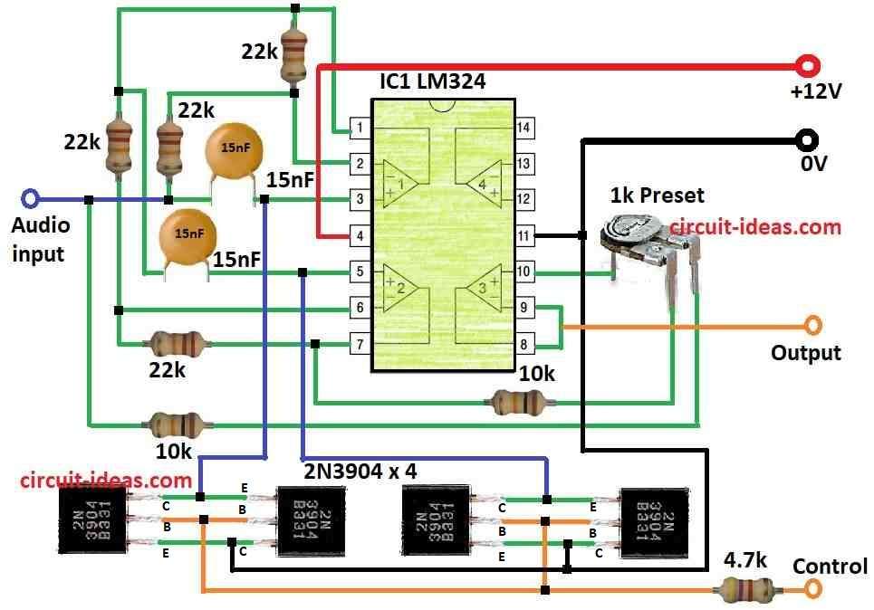
Parts List:
| Components | Quantity |
|---|---|
| Resistors ( All resistors are 1/4 watt) | |
| 22k | 4 |
| 10k | 2 |
| 4.7k | 1 |
| Preset 1k | 1 |
| Capacitors | |
| Ceramic 15nF | 2 |
| Semiconductors | |
| IC LM324 | 1 |
| Transistor 2N3904 | 4 |
To begin with, this circuit move the rejected sound frequency across 10kHz range using special notch filter; also where the notch goes depend on voltage given to control input.
Here, IC1 and IC2 work like all pass filters with flat sound across high frequency which is higher than what we can hear, but they make input and output signal shift in phase by 0.5 CR.
Also, this shift slowly goes close to 180 degree and when that happen the input and output cancel each other.
So this variable notch filter work like all pass notch filter which lets all sound go, except at 0.5 CR.
Moreover, two transistor circuits Q1, Q2 and Q3, Q4 act like voltage controlled resistors and they help change notch frequency when control voltage changes.
Formulas:
The parts connected to the input and output pins power the LM324 IC; here are some formulas that make the op-amp circuit work:
If we use the LM324 IC as an inverting amplifier, it follows this formula:
Vout = – (Vin * R2) / R1
here:
- Inverting input connects to ground using resistor R1.
- Resistor R2 goes from output to inverting input.
Non-Inverting Amplifier:
If it is non-inverting type then use this formula:
Vout = Vin (1 + R2 / R1)
here:
- Inverting input connect to ground using R1.
- Resistor R2 goes between non-inverting input and output.
Differential Amplifier:
For differential amplifier formula is more hard and it depends on circuit design.
Important to Know:
These formulas work if op-amp is perfect, like it has big gain and no input error voltage, but actual circuit is not perfect but some small changes can happen in output.
Also, LM324 IC have 4 op-amps inside so we can use these formulas to make 4 amplifier circuits.
Therefore, if we want to do more than just amplify like filter or oscillate we need to see full circuit diagram and follow the design rules.
How to Build:
To build a Variable Notch Filter Circuit follow the below mentioned steps for connections:
Assemble the Parts:
- First, collect all needed parts. Use the circuit diagram to see which parts we need and check the values for resistors, capacitors and other parts and ensure they match the diagram.
Get the Diagram:
- Next, find the circuit diagram for variable notch filter and we can look online or check electronics books.
- Also, the diagram will show how to connect the parts and what values to use.
Setup on PCB or Breadboard:
- After that, prepare a PCB or breadboard to build the circuit and put all parts on the breadboard just like in the diagram and use jumper wires to connect them.
Op-Amp Setup:
- Here, IC1 and IC2 are op-amps, so set them up as shown in the diagram, connect the positive and negative pins correctly and make sure the power supply has proper grounding.
Transistor Circuits:
- Then put transistors Q1, Q2, Q3 and Q4 in place like the diagram shows and also use them as voltage controlled resistors to change the notch frequency and check all connections are good.
Control Input:
- Now, connect a preset variable resistor to control input and this will also help us adjust the notch frequency.
Testing the Circuit:
- After that, turn ON the power and use an oscilloscope or signal generator with an audio amplifier to test and also watch how the notch frequency changes when we adjust the preset.
Tuning the Circuit:
- Also, if the notch frequency is not right change resistor or capacitor values or adjust the preset.
Final Touch:
- Finally, once everything works fine move the circuit to a permanent PCB and put it inside a box to keep it safe.
Keep Notes:
- Write down any changes we have made with resistor values, capacitor values, preset settings as this will help in future.
Important Tip:
- Lastly, always follow the circuit diagram carefully and double check with all the connections and if anyone is new to electronics then better to ask help from someone who knows it well.
Conclusion:
Overall, this Variable Notch Filter Circuit can block one sound frequency and let others go, also we can change the blocked frequency using control voltage.
Hence, this circuit is good for music and sound work and it is also easy to build if followed as per diagram.
For safety always check connections and test before use.
Leave a Reply