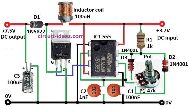
Boost Converter Circuit using IC 555 take low DC voltage and makes high DC voltage and is used for IC 555.
IC 555 make PWM signal to control other parts.
Other parts used are IRFZ44N, inductor, diode, resistor and capacitor.
Circuit Working:
Parts List:
| Component Type | Description | Quantity |
|---|---|---|
| Resistors | 1k ohm 1/4 watt | 1 |
| Potentiometer 47k ohm | 1 | |
| Capacitors | Ceramic 100nF | 1 |
| Ceramic 1nF | 1 | |
| Electrolytic 100μF 25V | 1 | |
| Semiconductors | IC 555 | 1 |
| MOSFET IRFZ44 | 1 | |
| Diode 1N4001 | 2 | |
| Diode 1N5822 | 1 | |
| Inductor coil 10uH | 1 |
Inductor does not gives energy fast.
First it store energy in magnetic field and then boost converter uses this energy to make high voltage by lowering current.
Current and resistance stay same only voltage changes.
Current in inductor is: I = V/R.
Inductor connect in series with voltage source and circuit turns ON and OFF again and again.
For fast switching we must use MOSFET with driver and switch is parallel with them.
Load and capacitor are in parallel to the circuit.
Diode between MOSFET and capacitor stop current from going back.
This circuit look like buck converter and sometimes called reverse buck converter.
Inductor try stop current change so input current stay steady.
So boost converter works like constant current source and the load get constant voltage.
IC 555 give PWM signal to N-channel MOSFET IRFZ44N.
Gate of MOSFET connect to IC pin 3.
Capacitor hold charge and gives stable output to load.
1. Charging Mode (Switch ON):
Light is ON and MOSFET is ON (activated).
Circuit completes the voltage across inductor.
Magnetic field is build around inductor.
All voltage go through MOSFET to ground with low resistance path.
Diode stop capacitor from discharging through MOSFET.
2. Discharging Mode (Switch OFF):
Switch OFF the path break.
Inductor makes voltage spike with surge and polarity flip.
The magnetic field collapses.
Energy from inductor goes through diode and charge capacitor and load.
Capacitor and source both gives power to load.
MOSFET IRFZ44N is main switch in this SMPS circuit.
Gate is driven by IC 555 and source to ground and drain does negative switching.
Formulas:
Below are some important formulas for boost converter:
1. Output Voltage:
Vout = Vin / (1 – D)
where:
- Vout is the output voltage
- Vin is the input voltage
- D is the duty cycle with value between 0 and 1
Duty Cycle:
D = Ton / T
where:
- Ton is when time switch is ON
- Tis the total time of one cycle
Inductor Current:
L * di/dt = Vin – Vout
where:
- L is the inductance
- di/dt is how fast inductor current is changing
Capacitor Voltage Ripple:
ΔVout = (Iout * Ton) / (C * f)
where:
- ΔVout is the voltage ripple in peak to peak
- Iout is the output current
- C is the capacitance
- f is the switching frequency
These formulas show how parts of boost converter work together.
How To Build:
To build a Boost Converter Circuit using IC 555 following are the below mentioned steps for connections:
- Pin 1 of IC 555 IC1 connect to ground.
- Pin 2 connect to pin 6 of IC1.
- Pin 3 connect to gate of MOSFET IRFZ44N.
- Pin 4 and pin 8 connect to positive power.
- Pin 5 connect to ground through capacitor C1.
- Pin 6 also connect to middle leg of 47k pot.
- Pin 7 connect to +3.7V input through resistor R1.
- Diode D2 go to top leg of pot from pin 7.
- Diode D3 goes to bottom leg of pot from pin 7.
- Capacitor C2 connect to pin 2 and 6 and then to ground.
MOSFET IRFZ44N:
- Gate connect to pin 3 of IC1
- Drain connect to +7.5V output
- Source connect to ground
- Capacitor C3 connect from +7.5V output to ground.
- Inductor coil and diode D1 connect to positive supply.
Conclusion:
This Boost Converter Circuit using IC 555 uses MOSFET switch and inductor to increase low voltage to higher voltage.
IC 555 give PWM signal to control the MOSFET.
Inductor stores energy and capacitor keep output voltage steady.
This small and easy circuit is good for when we need more DC voltage than what we have.