This DC to DC Adjustable Converter Circuit using IC TL497A works like small helper which can change voltage from power source.
Also, it takes a low input voltage and produces a higher output voltage, much like a small power adapter, furthermore, we can modify this circuit to operate in different ways, depending on the output voltage you need.
Hence, if we want small boost or big jump this circuit can do it, IC TL497A chip uses smart method called PWM to change voltage easy and save power.
Circuit Working:
Parts List:
| Components | Values | Quantity |
|---|---|---|
| Resistors | 1.5Ω | 1 |
| 10k | 1 | |
| 820Ω | 1 | |
| Potentiometer 10k | 1 | |
| Capacitors | Ceramic 0.47µF | 1 |
| Ceramic 0.1µF | 1 | |
| Electrolytic 47µF 40V | 1 | |
| Electrolytic 100µF 16V | 1 | |
| Semiconductors | IC TL947A | 1 |
| Coil inductor 40µH | 1 |
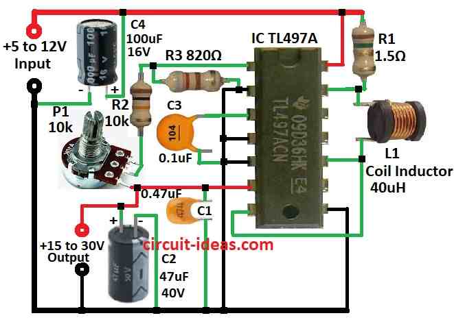
This voltage converter uses TL497A chip it take 5 to 12V input and makes higher voltage like 15 to 30V, which is very useful for mobile things where battery gives max 12V only.
Circuit uses TL497A like flyback converter with 40uH 2A coil and capacitor C2 and C1 help stop voltage spikes.
Max output current depend on how much input and output voltage is different which is around 100mA, ripple voltage is not so big.
Standby current is near 8mA and efficiency is around 70%.
Formulas:
From this circuit we can use basic flyback converter formulas, but to get exact result for actual design we need more checking and simulation.
TL497A chip is flexible but when use in flyback converter many parts and settings work together in complex way.
Here are some important formulas:
Duty Cycle D:
D = Vout / (Vout + Vin) × Np / Ns
where:
- Vout is output voltage
- Vin input voltage
- Np is number of turns in primary coil
- Ns is number of turns in secondary coil
Inductor Value L:
L = (Vin × D × Ton) / (ΔIpk)
where:
- Ton is time switch is ON
- ΔIpk is ripple of inductor current from peak to peak
- Output Voltage Ripple ΔVout:
ΔVout = Iout / (f × Cout)
where:
Note:
TL497A has built-in oscillator, driver and error amp so design is little bit easier, but still we need to check all component values and external parts carefully.
This is just short a summary but to make good flyback converter which need full design, test and balance many things and for more details better to check full datasheet and design guide.
How to Build:
To build a DC to DC Adjustable Converter Circuit using IC TL497A follow the below mentioned steps:
Schematic Design:
- First, make circuit diagram using TL497A chip like in datasheet and then choose parts to get output voltage between 15 to 30V and max current 100mA.
PCB Layout:
- Next, draw PCB board using circuit and put parts in good place to stop noise and be sure all circuit parts work good.
Component Placement:
- After that, solder all parts on PCB like a circuit diagram and be careful with parts that have direction like capacitors and diodes.
- Use power supply with input from 5V to 12V, check output voltage with multimeter and it should be 15 to 30V and also check output current.
Fine-tuning:
- If output is not correct change some part values or settings to fix voltage and current.
Enclosure:
Final Testing:
- Now, do last check to be sure converter works perfect and is reliable.
Note:
- Always follow TL497A datasheet and tips to choose right parts and make safe and good design.
Conclusion:
Overall, DC to DC Adjustable Converter Circuit using IC TL497A chip is good and flexible, as it can change low voltage to high voltage easy and work nice.
Moreover, we can use it in many applications and we can adjust the output voltage.
Therefore, it works well for devices such as mobile electronics, car electronics and other battery-powered systems.
TL497A also have good things like voltage control and protection from too much current; so it help to make strong and stable power for many electronic devices.
Leave a Reply