Light is present all around us and photosensitive devices can feel this light, as these are very useful electronic components which change their action when light falls on them.
We use these devices in automatic lights, alarms and many other electronic circuits.
In this article, for Understanding Photosensitive Devices Circuits we will learn about their uses in daily life; and how it can turn ON or OFF lamp, alarm or control system.
Photocell:
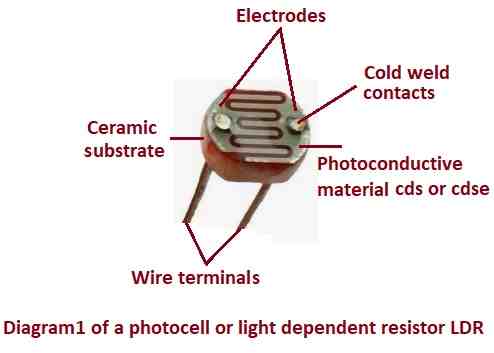
Manufacturers place a light-sensitive material in a zigzag pattern between two metal contacts on a ceramic base.
Zigzag gives is more contact area and material is mostly CdS or CdSe, also thickness and width change resistance and performance.
All parts are inside metal or dark plastic case with clear window.
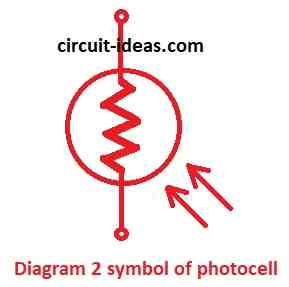
Diagram 2 shows symbol of photocell.
Photocell Light Switches:
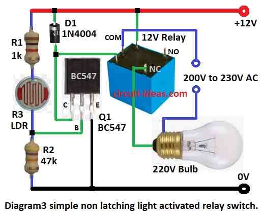
Diagram 3 to 8 show light switch circuit with photocell and relay.
Diagram 3 shows a simple circuit that works well in dark places such as cabinets.
Photocell R1 with resistor R2 make voltage divider for base of transistor Q1.
In dark the R1 has high resistance and there is no base voltage so Q1 is OFF and so relay also OFF.
In light the R1 has low resistance and then base gets voltage so Q1 is ON and relay also is ON, which can control other circuit.
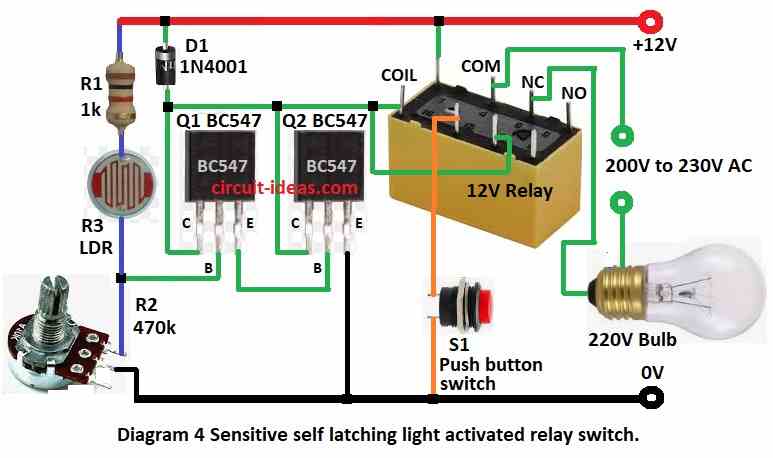
Diagram 3 has simple sensitivity and diagram 4 is more sensitive.
Here, two transistors Q1 and Q2 are in Darlington pair and potentiometer R2 to adjust better.
It can also lock itself ON using with extra relay contact and pushbutton S1 (NC) reset the circuit.
Diagram 5 shows how photocell work in this circuit.
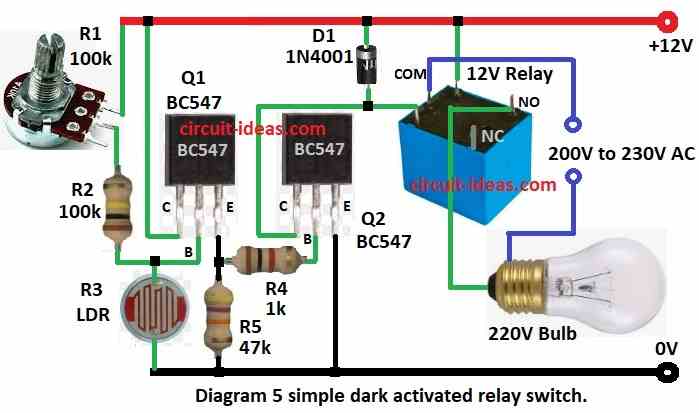
R2 and photocell R3 make voltage divider and when light is low the voltage at R2–R3 point goes high and then this voltage goes to Q1 emitter follower.
Then it goes through R4 to Q2 amplifier and then Q2 drives the relay.
In diagram 4 and 5 the light trigger can change if voltage or heat changes.
Diagram 6 is more stable and it works same even if voltage or heat changes.
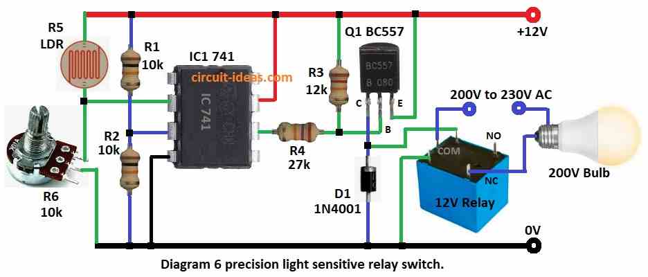
In this circuit R5 photocell, R6 potentiometer, R1 and R2 make Wheatstone bridge and IC1 op-amp with Q1 transistor and relay work as sensitive switch and they check balance of bridge.
Bridge is stable and it does not change by voltage or heat, but it only changes when light changes value of parts.
Diagram 7:
Add small hysteresis to stop relay from fast ON/OFF near trigger point.
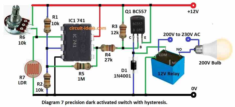
The relay turns on in low light and stays on until the light becomes brighter and this gap is called hysteresis.
Bigger R5 means more hysteresis and no R5 then no hysteresis.
Diagram 8 uses two op-amps for precise light and dark control.
Relay ON when light above one level or below other level and R1 set dark level and R3 set bright level.
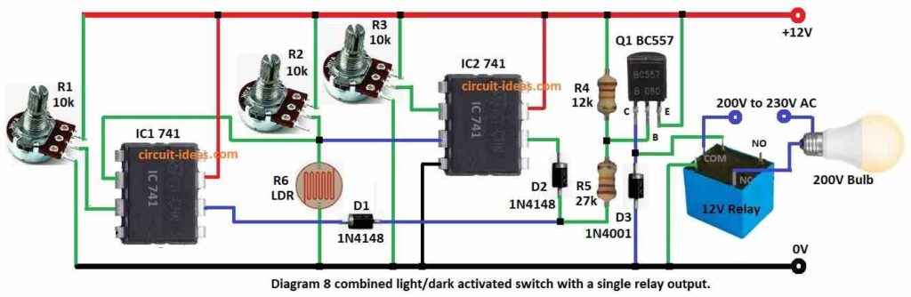
In diagram 6 and 8 circuits the potentiometer value should be same as photocell resistance in normal light and this makes circuit work better when relay turns OFF.
Photodiodes:
Photodiodes are light sensors and they work by photoelectric effect.
When light falls on them, they produce a small electrical signal.
Manufacturers make them from silicon, germanium, or gallium arsenide.
They have PN junction and when light hits the electrons move then electron hole pairs form and electric field separates them.
Hence, this makes photocurrent matching the light level.
Like solar cells, they generate voltage in light but however, circuits use them in reverse bias for faster and more sensitive operation.
Sensitivity depends on the light wavelength and the materials bandgap and they are also reliable, efficient and widely used in light detection systems.
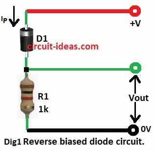
In reverse bias a normal silicon diode see diagram 1 only has tiny leakage current, so no voltage appears across resistor R1.
If we remove the case and expose the PN junction then we can put it back in circuit and it reacts to light.
When light hits diode current goes higher to about 1 mA and then voltage appears across R1.
All silicon PN junctions can sense light and also a photodiode is just normal diode with clear cover so light can enter.
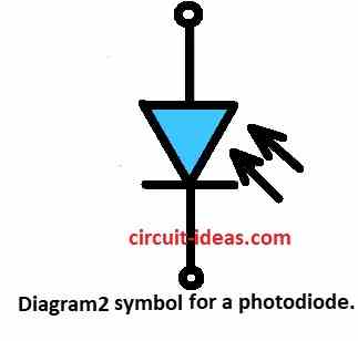
Diagram 2 shows symbol of photodiode.
In Diagram 3 photodiode is in reverse bias.
Here, the circuit measures the output voltage across load resistor R1, which connects in series with the photodiode.
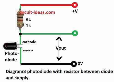
This resistor can also connect between diode and ground same as in diagram 1.
Photodiodes respond to different light wavelengths and response depends on material used in semiconductor.
Diagram 4 shows normal response curve for silicon light sensors and it includes both photodiodes and phototransistors.
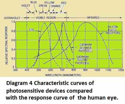
Silicon photodiodes are less sensitive to visible light than CdS or CdSe photocells, but they react much faster to light changes.
CdS and CdSe photocells are good for visible light and they have slow response and can connect directly.
Photodiodes are better for infrared (IR) and they give fast response and can handle AC signal.
Also, designers use it in IR remotes, beam-break switches, and alarm systems.
PbS (lead sulfide) photocells work same as visible light types, but they respond only in infrared range.
Phototransistors:
Phototransistor is special part that senses light and makes stronger signal., it works like mix of photodiode and transistor.
When light hits it, it generates a small current, the circuit then amplifies this current to detect even tiny changes in light.
It is normal BJT or FET changed to react to light.
Usually it has 2 pins collector and emitter or 3 pins collector, emitter and base.
Also, expose the base to light, and photons generate charges that make current flow.
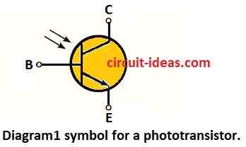
Diagram 1 shows phototransistor symbol and it is silicon NPN transistor with clear case so light reach PN junction.
Usually leave the base pin open, as shown in Diagram 2.
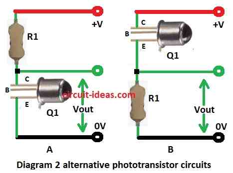
Diagram 2A shows base, collector junction in reverse bias and it works same as photodiode.
When light falls current forms in base, collector area and this current goes into base.
Then it is amplified and comes out as collector current.
Resistor R1 changes this current into output voltage.
The collector and emitter currents are almost equal, while the base remains open without feedback.
Diagram 2B works same as 2A and here output voltage is across R1 from emitter to ground.
Phototransistors are about 100 times more sensitive than photodiodes, but they are slower up to few hundred kHz.
Photodiodes are faster and can work up to tens of MHz.
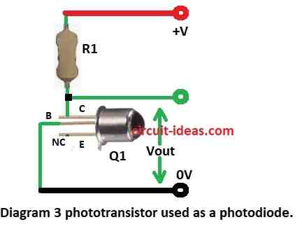
Also we can change phototransistor into photodiode by wiring as in diagram 3.
Another way to say it: we can change sensitivity and speed of phototransistor by using potentiometer.
Connect potentiometer between base and emitter as in diagram 4.
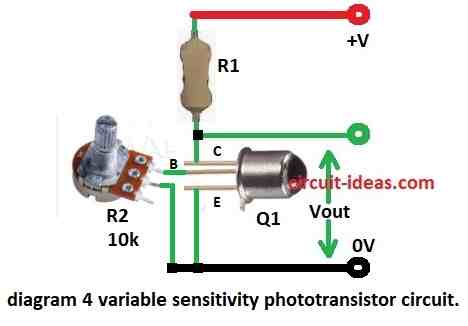
Without R2, the phototransistor works normally and with R2, it behaves more like a photodiode.
In Diagrams 2 to 4, R1 provides the proper balance.
Higher R1 gives more voltage gain but lower bandwidth and R1 must keep photosensor in linear range.
Darlington phototransistor uses two transistors together.
See diagram 5.
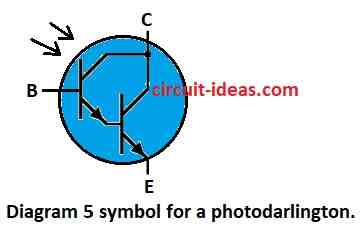
Darlington phototransistors are about 10× more sensitive than normal type, but they are much slower. and they work only up to tens of kHz.
Conclusion:
Overall, this project for Understanding Photosensitive Devices Circuits is easy to learn, as photosensitive devices work with light.
Furthermore, circuit changes output when light increase or decrease and it is useful in making automatic lights, alarms and sensors.
Leave a Reply