Photosensitive devices are parts or systems that react to light levels or energy.
They are used in many fields from gadgets we use every day to big industrial machines, because they can change light signals into electrical signals or start certain actions based on how bright the light is.
In this article, we will explore light sensitive devices and see how they can be applied in different control circuits.
Some examples of these devices are photocells, photodiodes and phototransistors.
Both visible and infrared light or even the lack of light can activate various circuits to control alarms, lights, motors, relays and other devices.
Light sensitive devices also known as photoelectric transducers change their electrical properties when they detect visible or infrared light.
Below are some functions and working for photocells, photodiodes and phototransistors devices.
Photocell:
Photocells are known by several names such as photoconductive cells light dependent resistors LDRs, and photoresistors.
They act as variable resistors with a huge range of resistance values that can change based on how much light hits them.
When it is dark the resistance is really high, but when it is bright the resistance drops significantly.
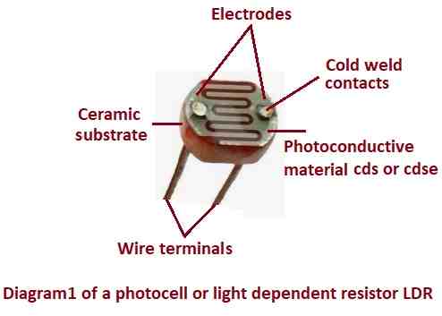
In diagram 1, you can see a view of a typical photocell.
It shows the special pattern of photoconductive material placed in a serpentine slot between two electrodes on a ceramic base.
This design helps to increase the contact between the photoconductive material and the metal electrodes nearby.
The materials used for the photoconductive part are usually cadmium sulfide CdS or cadmium selenide CdSe.
The choice of material along with how thick and wide it is, affects the resistance and power rating of the photocell.
The whole assembly is usually housed in a metal or dark plastic case with a clear glass or plastic window covering the photoconductive material.
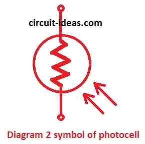
Diagram 2 shows the schematic symbol for the photocell.
Photocells come in different sizes ranging from about one eighth of an inch 3 mm to more than one inch 25 mm in diameter.
The most common ones are around three eighths of an inch 10 mm.
Smaller photocells are great for tight spaces like in card readers, but they do not handle a lot of power.
Some of these devices are sealed tightly to protect them from tough conditions.
Photocell Light Switches:
Diagram 3 to 8 show different light activated switch circuits that use a photocell and relay contacts.
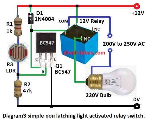
The basic circuit in diagram 3 is made to respond when light enters a usually dark area like inside a cabinet or closet.
The photocell R1 and resistor R2 work together to create a voltage divider that controls the base bias of Q1.
When it is dark the photocell has high resistance meaning no bias reaches the base of Q1, so both Q1 and the relay are off.
However, when enough light hits the photocell, its resistance decreases allowing bias to reach Q1.
This turns on relay which can then control other circuits.
Formulas:
Formulas for simple non latching light activated relay switch circuit:
Voltage Divider Formula (Across LDR and R3):
The LDR and resistor R3 form a voltage divider.
The voltage across the LDR, VLDR is given by:
VLDR = RLDR / RLDR + R3 * Vin
where,
- RLDR is the resistance of the LDR varies with light intensity
- R3 is the resistor value in ohms
- Vin is the supply voltage
LDR Resistance Formula:
The resistance of the LDR changes in the opposite way to the amount of light, you can estimate it like this:
RLDR ∝ 1 / Light Intensity
The exact behavior depends on the LDR characteristics, which is provided in a datasheet.
Base Current (IB) of Transistor:
The current that flows through R2 is called the base current and the voltage drop across the base emitter junction is usually about 0.7 volts for silicon transistors.
IB = VLDR − VBE / R2
Collector Current (IC) of Transistor:
The collector current is related to the base current by the transistors current gain (β):
where,
- β is the current gain of the transistor which is in datasheet.
Relay Activation Condition:
For the relay to activate:
IC > IRelay
where,
- IRelay is the minimum current required to energize the relay coil.
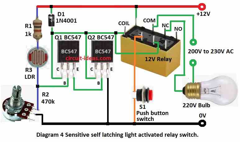
Diagram 3 has a way to adjust sensitivity but diagram 4 shows how to fix its low sensitivity by using Darlington coupled transistors Q1 and Q2 instead of just Q1 along with a potentiometer R2 for better sensitivity control instead of a fixed resistor.
The diagram also explains how to make the circuit self latching with another set of relay contacts.
A normally closed pushbutton switch S1 allows the circuit to be reset when needed.
Formulas:
Formulas for sensitive self latching light activated switch circuit:
Voltage Divider Formula for LDR and Resistor:
The LDR and resistor R2 form a voltage divider.
The output voltage at the base of Q1 can be calculated as:
Vout = Vin × R2 / R2 + RLDR
where,
- Vin is the supply voltage 12V.
- RLD is the resistance of the LDR, which changes with light intensity.
- R2 is the fixed resistor 470k
LDR Resistance:
The resistance of the LDR depends on the light intensity and can be calculated by:
RLDR = k × Lux − n
- k and n are constants dependent on the LDR.
- Lux is the intensity of light in lumens per square meter.
Base Current for Transistor Q1:
For Q1 to turn on, its base emitter voltage (VBE) must reach approximately 0.7V. The base current can be calculated using:
IB = Vout−VBE / R1
where,
- R1 is the base resistor 1k.
- VBE is the base emitter voltage around 0.7V for BC547.
Collector Current for Q1:
The collector current IC is related to the base current by the transistors current gain hFE:
IC = hFE × IB
Relay Activation:
The relay coil requires sufficient current to activate.
The current flowing through the relay coil is provided by Q2 when it is turned on.
The relays current can be estimated by:
Irelay = Vcoil / Rcoil
where,
- Vcoil is the voltage across the relay coil 12V
- Rcoil is the coil resistance specified by the relay datasheet
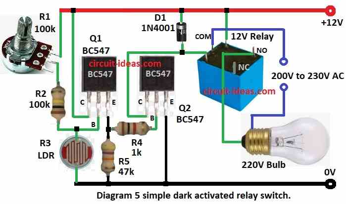
Diagram 5 demonstrates how a photocell can create a simple relay that activates in the dark when the light level drops below a certain point set by potentiometer R1.
Resistor R2 and photocell R3 form a voltage divider and as the light decreases the voltage at the R2, R3 junction rises.
This voltage which is buffered by emitter follower Q1 controls relay through a common emitter amplifier Q2 and a current limiting resistor R4.
The light trigger levels in the circuits shown in diagram 4 and 5 can change based on the supply voltage and the surrounding temperature.
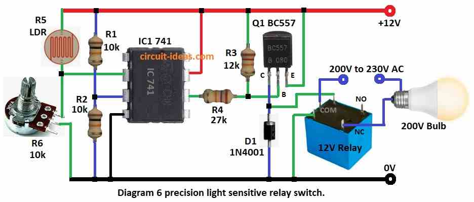
However, diagram 6 presents a very precise light activated circuit that remains unaffected by these changes.
In this setup the photocell R5 potentiometer R6 and resistors R1 and R2 are arranged to create a wheatstone bridge.
The operational amplifier op amp ICI along with the transistor Q1 and relay work together as a super sensitive switch that detects balance.
The balance point of the bridge does not change with variations in supply voltage or temperature, it only reacts to changes in the values of the components in the bridge.
In diagram 6, the photocell R5 and potentiometer R6 make up one side of the bridge while R1 and R2 form the other side.
These sides can be thought of as voltage dividers.
The R1 R2 side provides a steady half supply voltage to the non inverting input of the op amp while the photocell and potentiometer divider gives a light dependent voltage to the inverting input of the op-amp.
To operate this circuit you need to adjust potentiometer R6 so that the voltage across the photocell and potentiometer is just slightly higher than the voltage across R1 and R2 when the light intensity reaches the desired level.
When this happens the output of the op amp goes to negative saturation, which activates Q1 and turns on the relay.
If the light intensity drops below that level the op amp output switches to positive saturation turning off Q1 and the relay.
This circuit is incredibly sensitive and can respond to very small changes in light.
Changes in light levels that are too tiny for our eyes to notice can be detected by a special circuit.
This circuit can be adjusted to work as a precise switch that turns on in the dark by switching the positions of the inverting and non inverting input pins of the operational amplifier op amp or by swapping the photocell with the nearby potentiometer.
Formulas:
Formulas for precision light sensitive relay switch circuit:
LDR and Resistor Divider Voltage
The LDR forms a voltage divider with R5 generating a voltage at the non inverting input of the op-amp:
V+ = R5 / R5 + RLDR × Vsupply
where,
- RLDR is the resistance of the LDR varies with light intensity
- R5 is the fixed resistor
- Vsupply is the supply voltage for 12V in the circuit
Reference Voltage
The reference voltage is set at the inverting input of the op-amp using R2 and R6:
V− = R6 / R2 + R6 × Vsupply
Transistor Base Current
When the op-amp output is high, it drives current into the base of Q1 BC557:
IB = Vop − amp − VBE / R3
- Vop−amp is the op-amp output voltage
- VBE is the base-emitter voltage of Q1 which is around 0.7V for BC557
- R3 is the base resistor
Relay Activation
The collector current of Q1 activates the relay:
IC = β × IB
where,
- IC is the collector current
- β is the current gain of the transistor BC557
The relay coil is activated if IC is sufficient to meet its current requirements.
Diode Protection
The diode D1(1N4001) protects the circuit from back EMF generated by the relay coil:
VD1 = −L dI / dt
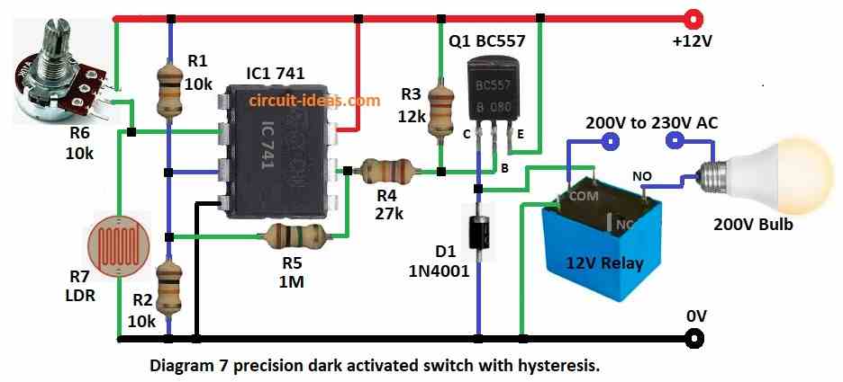
In the circuit shown in diagram 7, a little bit of hysteresis can be added using the feedback resistor R5.
This means that the relay will turn on when the light drops to a certain level, but it wont turn off until the light gets much brighter than that level.
The amount of hysteresis depends on the value of R5, if R5 is disconnected there is no hysteresis at all.
Diagram 8 illustrates how to create a precise light/dark switch by combining light and dark switches using op-amps.
This switch will activate relay when the light goes above one set level or drops below another set level.
Potentiometer R1 adjusts the dark level while potentiometer R3 can be set to make turn on at the brightness you want.
In the circuits shown in diagrams 6 to 8 the resistance values of the series potentiometers should match the resistance values of the photocell at the normal light level for each circuit.
Formulas:
Formulas for combined light dark activated switch with a single relay output circuit:
Light Detection Using LDR (IC1):
The LDR changes its resistance based on light intensity.
The voltage at the non-inverting terminal of IC1 is determined by the voltage divider formed by R6 LDR and R2.
Voltage at non-inverting terminal (+) of IC1:
V+ = (R2 / (R2 + R6)) * Vcc
where,
- R6 is the resistance of the LDR.
- Vcc is the supply voltage 12V.
The reference voltage at the inverting terminal (-) is adjustable using R1.
Transistor Switching (Q1)
The output of the op-amps controls Q1 BC557 PNP transistor, which in turn activates the relay.
Base Current for Q1:
IB = IC / hFE
where,
- IC is the collector current equal to the relay current approx 50 mA for a 12 V relay.
- hFE is the current gain of the transistor around 100 for BC557.
Collector Current for Relay Activation:
IC = (Vcc – VCE(sat)) / RL
where,
- VCE(sat) is the saturation voltage of the transistor around 0.2V.
- RL is the resistance of the relay coil.
- Relay Diode Protection D3
The diode D3 protects the transistor from the back EMF generated by the relay coil.
Photodiodes:
Photodiodes are special types of semiconductor devices that can sense light.
They are part of a group called photosensitive devices.
These devices work by using the photoelectric effect which means that when light hits them, they create an electrical signal.
Photodiodes are usually made from materials like silicon Si, germanium Ge or gallium arsenide GaAs.
They have a special part called a PN junction that lets light in through a clear window or lens.
When light hits the photodiode, it makes electrons in the semiconductor material move creating pairs of electrons and holes.
The electric field in the PN junction helps separate these carriers which leads to a photocurrent that matches the lights brightness.
Just like solar cells photodiodes produce a voltage when they are in the light.
They work in a reverse biased mode allowing for quick response times and better sensitivity.
How sensitive a photodiode is depends on the lights wavelength, which is linked to the semiconductors bandgap.
Because of their reliability and efficiency in turning light into electrical signals photodiodes are important in todays electronics and optical systems.
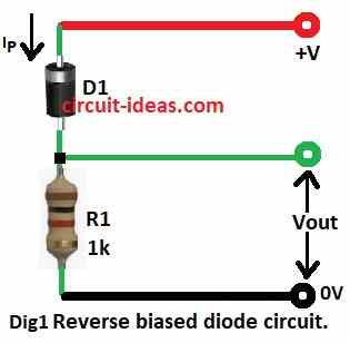
When a regular silicon diode is set up in a reverse biased circuit like in diagram 1 only a small leakage current will pass through it and there wont be any voltage across resistor R1.
But if you take the case off a regular silicon diode to show its PN junction and put it back in the same circuit, you can see its ability to respond to light.
When light hits the diode the current can increase to about one milliampere which creates a voltage across R1.
All silicon PN junctions can sense light so a photodiode is basically a regular silicon PN junction diode that has a clear cover to let light in.
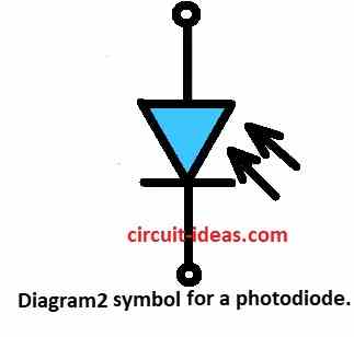
Diagram 2 shows what its standard symbol looks like.
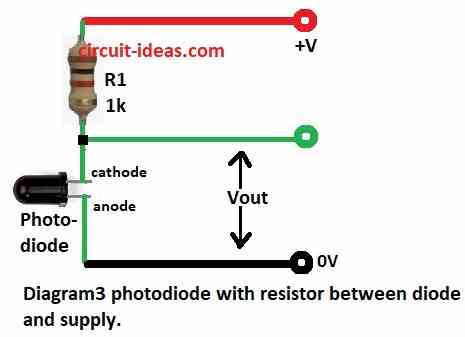
In diagram 3, the photodiode is reverse biased and the output voltage is measured across a load resistor R1 that is connected in series.
This resistor can also be placed between the diode and the ground just like in diagram 1.
Photodiodes have specific responses to different light wavelengths, which depend on how the semiconductor material is treated.
Diagram 4 shows a typical response curve for all silicon photoreceptors, which includes both photodiodes and phototransistors.
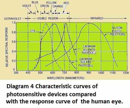
While silicon photodiodes are not as sensitive to visible light as cadmium sulfide or cadmium selenide photocells, they react more quickly to changes in light.
Cadmium sulfide and cadmium selenide photocells work best in visible light applications where they are directly connected and slower response times are okay.
On the other hand photodiodes are more effective in the infrared range where they can pick up AC signals and need to respond quickly.
Photodiodes are often found in things like infrared remote controls beam interruption switches and alarm systems.
On the other hand lead sulfide PbS photocells work similarly to visible light photocells but they only operate in the infrared part of the light spectrum.
Phototransistors:
A phototransistor is a special device that can sense light and also boost electrical signals kind of like a combination of a light sensitive photodiode and a transistor.
When light hits the phototransistor, it creates a small electric current which gets amplified so the device can detect even tiny changes in light.
Basically, a phototransistor is a modified version of a bipolar junction transistor BJT or a field effect transistor FET that can respond to light.
It typically has either two terminals called collector and emitter or three terminals collector, emitter and base.
In these devices the base area is designed to catch light and the light particles or photons help create charge carriers.
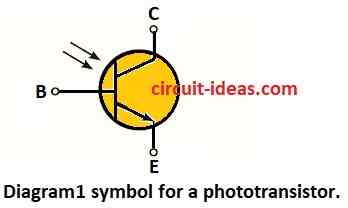
Diagram 1 displays the standard symbol for a phototransistor.
A phototransistor is a type of silicon bipolar NPN transistor that comes in a case with a clear cover allowing light to reach its PN junctions.
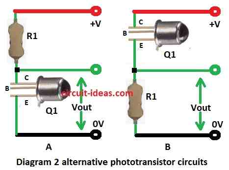
Typically, the base pin is left open as illustrated in both parts of diagram 2.
In diagram 2A the base collector junction is reverse biased making it function like a photodiode.
The light creates currents in the base collector junction which then flow into the base of the transistor.
This process amplifies the current resulting in a collector current that serves as the output.
The amplified current across resistor R1 generates the output voltage.
The collector and emitter currents of a phototransistor are usually quite similar because the base is not connected meaning there is no negative feedback.
Therefore, the alternative circuit in diagram 2B performs almost the same as the one in diagram 2A.
The output voltage is measured across R1 which connects the emitter to the ground.
Phototransistors are generally about one hundred times more sensitive than photodiodes, but they can only operate at a maximum frequency of a few hundred kilohertz which is much lower than the tens of megahertz that photodiodes can handle.
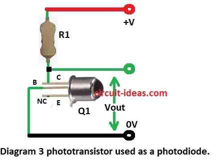
You can turn a phototransistor into a photodiode by connecting it as shown in diagram 3.
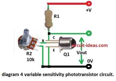
A different way to explain this is that you can change how sensitive and fast a phototransistor works by connecting a potentiometer between its base and emitter like in diagram 4
If you leave R2 disconnected the phototransistor works normally, if you connect R2, it acts like a photodiode.
In real life uses of the circuits in diagram 2 to 4 the value of R1 is usually picked as a balance because while increasing R1 can boost voltage gain it also reduces the useful operating bandwidth.
Plus, in many cases R1 needs to be set to make sure the photosensitive device works in its linear range.
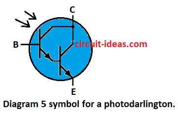
Darlington phototransistors are made up of two transistors connected together, as shown in diagram 5.
They are about ten times more sensitive than regular phototransistors but they can only operate at maximum frequencies in the tens of kilohertz range.
Conclusion:
Photosensitive devices such as photodiodes, phototransistors and photovoltaic cells are super important because they change light into electrical signals.
This ability allows them to be used in many different technologies and in our daily lives.
They work by using the way light interacts with special materials called semiconductors, which helps them do things like detect light, take pictures and collect energy.
Leave a Reply